KULeuven Course EMC
PCB Design and Layout Techniques for Cost-Effective SI, PI and EMC, in 2015
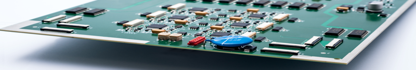
![]() The research group ReMI (Reliability in Mechatronics and ICT) organizes a course on basics and advanced PCB design and layout techniques.
The research group ReMI (Reliability in Mechatronics and ICT) organizes a course on basics and advanced PCB design and layout techniques.
Every two years, on average, every type of semiconductor that is available on the market goes through a die-shrink, which makes their emissions and immunity worse. This applies to older device types, like 74-series TTL and HCMOS, as well as to the latest microprocessors and memories, so designing with the same old parts does not protect us from this problem.
So PCB technology must continually advance, to design PCBs in a way that doesn’t create problems for Signal Integrity (SI), Power Integrity (PI) and ElectroMagnetic Compatibility (EMC).
Advanced PCB EMC techniques are generally needed when resonances in PCB structures are excited by the frequencies present in the analogue, digital or power supply current waveforms.
After the appropriate choice of semiconductors (or designing your own ASICs), the most cost-effective SI, PI and EMC techniques are those applied at the PCB level.
This course provides a practical grounding in PCB EMC design and layout techniques that have been proven over many years in real life to help companies quickly improve their commercial and financial performance by:
- Bringing products to market more quickly
- Improving functional performance
- Reducing overall unit manufacturing costs
- Easily complying with legal EMC requirements
- Reducing warranty costs and improving customer perception of the brand
- Reducing financial risks
- Improving Return On Investment
Click here for more info.
This course is divided in two days and includes following topics
Day 1:
- The scope of these layout techniques
- Saving time and money
- Segregation
- Interface analysis, filtering, and suppression
- 0V and power planes
- PCB-chassis bonding
- Power supply decoupling
- Switch-mode power converter layout (AC-DC, DC-DC, etc.)
- Transmission line techniques
- Layer stacking
- Devices with BGA packages and/or multiple DC rails
- Some useful references and sources
Day 2:
- When should we use advanced PCB techniques?
- Future trends and their implications
- Rules of thumb, approximations, simulations
- Virtual design for SI, PI and EMC
- Advanced segregation techniques
- PCB-level shielding up to GHz
- Advanced interface filtering and suppression
- Advanced PCB-chassis bonding
- Advanced PCB planes
- The totally shielded PCB assembly
- Advanced PCB decoupling
Both days are programmed as follows:
- 09:00-10:30 Part 1
- 10:30-10:45 Coffee break
- 10:45-12:15 Part 2
- 12:15-13:00 Lunch
- 13:00-15:00 Part 3
- 15:00-15:30 Coffee break
- 15:30-17:00 Part 4
Click here to subscribe.
- €750 (excl. VAT) for all modules, free book “EMC for Printed Circuit Boards – Basic and Advanced Design and Layout Techniques by K. Armstrong” included!
- In combination with the course "Electromagnetic compatibility: mysteries unraveled..." a reduced price of €1200 (excl. VAT)
A 10% discount applies for members of Agoria or the NEATH project. The participation fee includes the lunch and coffee break